본문
Nano·Micro Structure Chip Design & Manufacture(OEM/ODM)
Design & Modeling
Optimized design and analysis of fluid flowing models and structures of chambers, channels, inlets, outlets, etc.
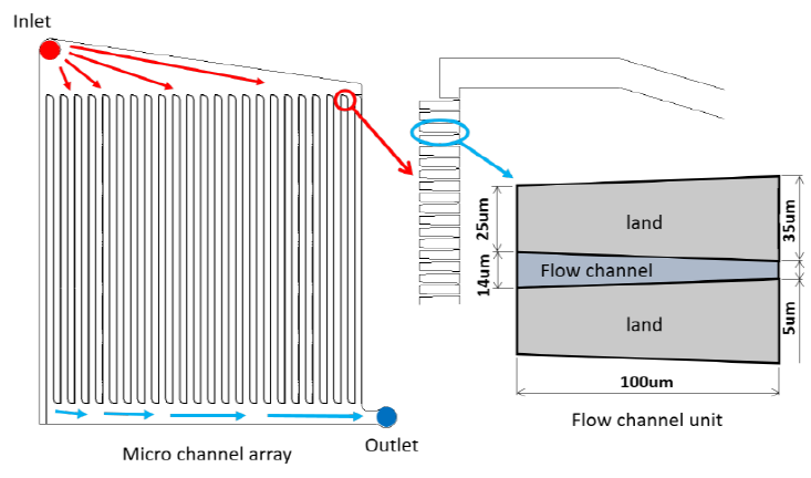
A Micro-Channel Design of a High Throughput Micro-fluidic Device for Screening Circulating Tumor Cells from the Blood Sample
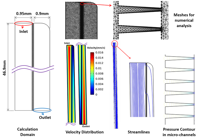
Numerical flow analysis for optimization of the micro-fluidic channel design to enhance the throughput of the fluid sample and the uniformity of the flow
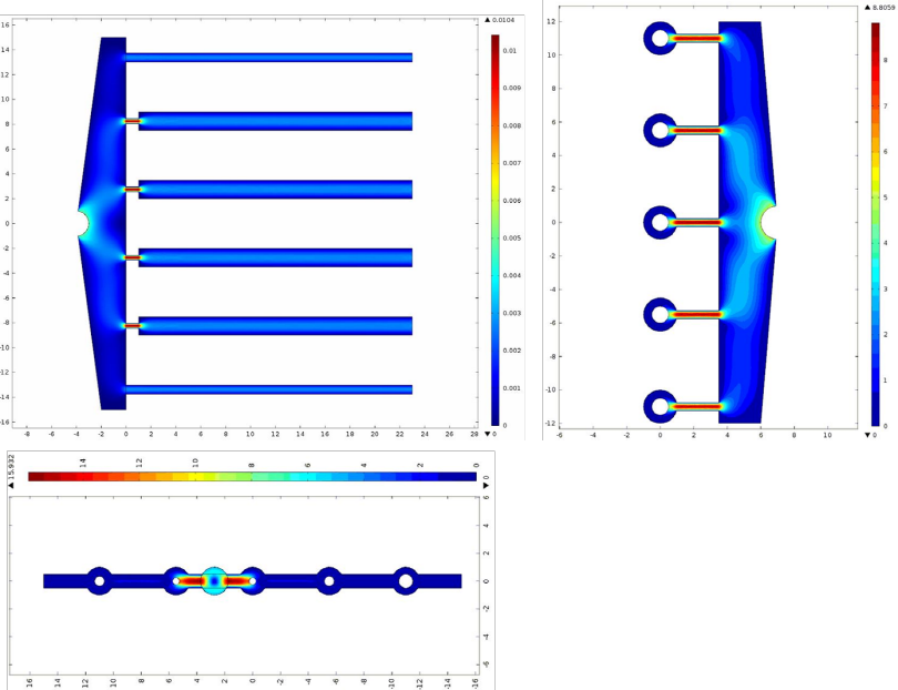
Numerical flow analysis and design optimization for the manifold of the multi-layer micro-fluidic device to deliver fluid sample uniformly to the micro-channels
Nano·Micro Patterned Stamper
Manufacturing nano/micro patterned molds utilizing MEMS technologies.
Core technology
Micro/nano patterns are transferred onto Si-wafer or Quartz by using semiconductor processes such as photolithography, scanner, laser direct writing, and Ni plating is performed according to the applications to provide Ni base molds.
Specifications
Pattern size: 100nm ~ hundreds of μm, aspect ratio < 3
Pattern shape: Pillar, Grating, Pinhole, Channel, etc.
Materials: Si-wafer, Quartz, Sodalime glass, Metal, etc
Application
microfluidic platforms for point-of-care testing, anti-reflective structures ect
Nano·Micro Injection Molding
Microfluidic channels or MEMS based nano/micro platforms in polymers can be injection molded.
Core technology
Mass production of sophisticated plastic products such as microfluidic channels with higher productivity and yield by applying highly-precise molds equiped with rapid heating & cooling system.
Specifications
Pattern size: 100nm ~ hundreds of μm, aspect ratio < 5
Pattern shape: Pillar, Channel, etc.
Processing area: 30mm×30mm ~ 400mm×400mm
Materials: PMMA, PC, PP, COC, TPU, etc.
Heating & cooling systems on molds
Application
Microfluidic channels for various in-vitro diagnostic and point-of-care testing devices
Bio-MEMS
liposome synthesis device
Assembly-Packaging
Packaging technology for plastic-plastic, film-plastic, plastic-wafer, and film-wafer is the finishing process of injection molded parts. It shows excellent sealing and bonding properties, which has been technologically invested by Korea Institute of Machinery & Materials as follows.
Package way
Packaging by Ultrasonic Welding & Mechanical Contact
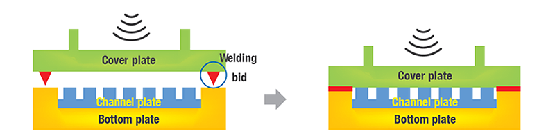
Hermetic sealing
Good adhesion
Good success rate(> 95%)
Good productivity (cycle time ~ 15 sec)
Packaging by Film Thermal Lamination
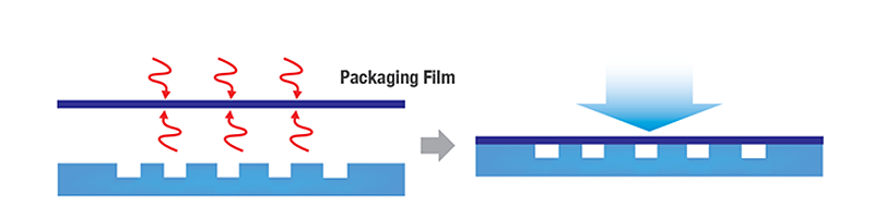
Typical packaging for microfluidic platforms currently
Good for a handy device
A Reversible Packaging Solution
Uniform contact pressure at the interface
Hermetic sealing
Controllable sealing level during operation
Excellent success rate(~ 100%) and productivity (< a few seconds)
Very short lead time for packaging
Application
Packaging for microfluidic channel based devices, and MEMS or Bio-MEMS based devices