본문
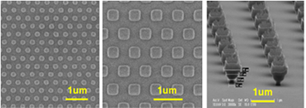
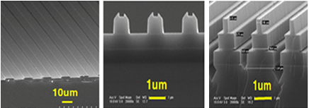
Nano·Micro Patterned Stamper
Manufacturing nano/micro patterned molds utilizing MEMS technologies.
Core technology
Micro/nano patterns are transferred onto Si-wafer or Quartz by using semiconductor processes such as photolithography, scanner, laser direct writing, and Ni plating is performed according to the applications to provide Ni base molds.
Specifications
Pattern size: 100nm ~ hundreds of μm, aspect ratio < 3
Pattern shape: Pillar, Grating, Pinhole, Channel, etc.
Materials: Si-wafer, Quartz, Sodalime glass, Metal, etc
Application
microfluidic platforms for point-of-care testing, anti-reflective structures ect